
With almost three decades of experience in semiconductor development and leadership, Petr Kamenický has taken the helm of the Czech Semiconductor Centre. In this interview, he outlines his plans to sharpen the Centre’s service portfolio, build distinctive areas of expertise with European reach, strengthen links between research and industry, and lay the foundations for long-term continuity and greater financial self-sufficiency beyond 2029.
What path did you take through the semiconductor industry to your current position as Director of the Czech Semiconductor Centre? What experience do you bring to the role?
My journey through the semiconductor industry began almost thirty years ago, working directly on integrated circuit development. I started as an analogue designer and layout designer, in a role where you deal with the details of the chip itself. I gradually moved into leading technical projects, then managing a development group and international development teams.
Over the years, I had the opportunity to contribute to the development of a range of semiconductor products for the automotive industry and gained experience both in the technical side of development and in managing people, projects and product strategies. I led teams of dozens of engineers and later entire development organisations.
A significant part of my career was spent building and developing onsemi’s Brno development centre, which grew from several dozen to almost two hundred specialists during my tenure. Alongside managing development, I also worked on strategic planning, international cooperation and innovation programmes supported by the European Union.
I therefore come to the role of Director of the Czech Semiconductor Centre with a combination of technical, managerial and strategic experience. One advantage is that, over the course of my career, I have worked at practically every level of management – from chip designer through project and line management to leading large organisations. This gives me a strong understanding of the needs of researchers, developers, companies and academia, and enables me to help connect the different parts of the Czech semiconductor ecosystem.
What will be the first steps you want to focus on in your new role?
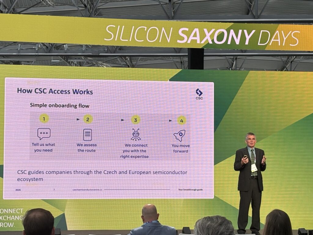
My first objective is to focus on the service catalogue of the Czech Semiconductor Centre and its partners. My primary concern is not the number or all-encompassing scope of the services, but their actual content and added value. It is not enough simply to be a place that knows whom to contact. Our objective must be to provide expert services based on genuine expertise that will have real significance for industry.
The Czech Semiconductor Centre coordinates a consortium of partners with exceptional potential. I see considerable scope for even deeper links between universities, research organisations and companies. Drawing on my many years of experience in industry, I look at the Centre’s services primarily through the eyes of the customer and their needs.
I am convinced that, together, we can build several areas of excellence in which the Centre and its partners will offer unique know-how. Such a base of expertise brings several positive effects: it attracts interest from industry and funding for further development, inspires new research directions with practical applications, and at the same time creates the conditions for innovation, spin-off companies and new business opportunities.
The foundation of everything, however, is the provision and development of genuine expertise based on the long-term and recurring needs of industry. Only in this way can we create services that remain relevant over the long term, benefit both companies and academia, and ultimately fulfil the Centre’s main objective, which is to develop the semiconductor ecosystem in the Czech Republic and the EU.
What, at the end of the project in February 2029, will be the most measurable proof that the Centre is working and has fulfilled its purpose?
I do not see the Centre as a one-off project with a fixed end date. I am pleased that the forthcoming European Chips Act 2.0 is moving in the same direction, envisaging the long-term development and continued operation of competence centres.
I will therefore regard the most measurable proof of success as the Czech Semiconductor Centre having a natural continuation beyond 2029. This will mean that it has succeeded in creating services for which there is genuine demand and which bring value to industry, academia and the entire Czech semiconductor community.
Ideally, it will no longer be a centre dependent solely on project funding, but one that can also rely on its own revenues and a degree of financial self-sufficiency.
In industry, the traditional indicators of success are turnover and profit. However, these usually reflect decisions made many years earlier. The true foundation of future success is the ability to create services and competencies that will remain attractive and in demand over the long term.
If we succeed in building areas of expertise that companies return to repeatedly, and if the Centre also demonstrates its added value through the volume of its own revenues, I will consider that very strong evidence that it is fulfilling its purpose. Not because its primary function is to generate profit, but because customers’ willingness to pay for services is the best confirmation of their genuine value.
At the end of 2029, I would not want to talk about the project having ended successfully. I would want to talk about the Centre continuing successfully.
Once you have addressed the update of the service catalogue, what other areas would you like to focus on?
Updating the service catalogue is one of my current priorities, but it is not a task that can be completed once and then left behind as we move on to something else. The service offering must remain dynamic and continue to evolve in response to the needs of industry and technological development. In a sense, the Centre’s activities will revolve around it over the long term.
However, if you are asking about my personal “passion project”, it is to build genuinely unique expertise in several carefully selected areas. I do not want the Czech Semiconductor Centre to be perceived merely as a coordinator or signposting service. I would like it to become a place to which companies and institutions from across Europe turn when they are seeking leading know-how in specific fields.
One area in which I see great potential, for example, is the use of artificial intelligence in design review processes for integrated circuit design. There are, of course, more such topics, but the common denominator is the effort to connect cutting-edge research with the practical needs of industry.
I would consider it a genuine success if the Czech Semiconductor Centre were approached not only by Czech companies, but also by customers and partners from other European competence centres. That would be clear evidence that we had succeeded in building expertise with European reach and reputation.

What makes the semiconductor ecosystem in Czechia unique compared with other European countries? What is our advantage?
I consider the interconnectedness of the Czech semiconductor ecosystem to be its greatest advantage. Although the Czech Republic is not one of Europe’s largest countries, this very fact gives us the opportunity to connect companies, universities, research organisations and public administration relatively quickly.
The close cooperation between the Czech Semiconductor Centre and the Czech National Semiconductor Cluster (CNSC) also plays a major role. Thanks to our close cooperation with CNSC, we have a direct link to the needs of industry as well as access to expert capacity. I regard this connection as one of our significant competitive advantages.
Another strength is the fact that the Czech Republic covers a surprisingly broad part of the semiconductor value chain – from research and integrated circuit design through the development of tools and software to certain areas of manufacturing, testing and advanced packaging. Although we are not the largest player in Europe, we have highly skilled experts and a long tradition, particularly in chip design and automotive applications.
Personally, however, I see openness and a willingness to cooperate as the greatest advantage. The Czech semiconductor ecosystem is large enough to possess significant competencies, while also being compact enough for key partners to reach agreement quickly and jointly move new initiatives forward.
What risks or obstacles must we take into account, not only in the context of the Czech semiconductor sector but also across Europe?
One of Europe’s greatest challenges is its ability to turn excellent research and innovation into successful industrial products. Europe has leading universities, research centres and talented experts, and very interesting technological ideas often originate here. Their commercialisation, however, is constrained by limited manufacturing capacity and often results in further development or production moving outside Europe.
Building modern semiconductor manufacturing capacity is extraordinarily demanding in terms of both capital and operations. Leading-edge manufacturing plants cost tens of billions of euros, and their economic sustainability depends heavily on high and sustained utilisation. This is why the issue cannot be resolved quickly or solely at the level of individual countries.
However, if Europe wants to strengthen its technological sovereignty and the resilience of its supply chains over the long term, it must retain at least the key parts of its manufacturing capacity within its own borders. Without them, it will be difficult to fulfil the ambition of maintaining control over its own semiconductor supply chain and becoming less dependent on geopolitical events in other parts of the world.
From the perspective of the Czech Republic, I see another important challenge in the ability to focus limited resources on areas in which we can genuinely excel. We cannot compete with everyone in everything. We must identify topics in which we can offer unique expertise and become a respected partner in the European ecosystem.
 How do you assess the Chips Act 2.0 proposal? And how do you see the future position of competence centres?
I view the Chips Act 2.0 proposal positively. Above all, this is because it builds on the idea of developing the European semiconductor ecosystem over the long term and does not view competence centres as one-off projects with a limited lifespan.
I consider it very important that Chip Competence Centres are envisaged as a permanent part of the European infrastructure supporting innovation, education and cooperation between industry and research. In my view, this is the right direction, because building expertise, trust and cooperation takes many years and cannot be achieved effectively through short-term projects.
A second significant aspect is the greater emphasis on bridging the so-called “valley of death”, the period between the creation of a successful prototype and its industrial deployment. Europe is very strong in research and development, but turning results into mass production and commercial applications is often the weakest link in the entire process.
From my perspective, this is one of the most important shifts compared with the first generation of the programme. Europe has already demonstrated that it can create cutting-edge technologies. It must now focus on ensuring that more of these technologies are transformed into real products and jobs created in Europe.
If research, pilot validation and subsequent industrial production can be linked more effectively, this could be of fundamental importance to the competitiveness of the European semiconductor industry.
Profile
Ing. Petr Kamenický has served as Director of the Czech Semiconductor Centre since mid-May 2026. He joins from onsemi, where he worked as a manager at the Brno R&D centre focused on chip design. He contributed to its growth from dozens of employees to around 180. He has more than 25 years of experience in automotive chip development, managing international teams and mixed-signal design. His work has focused on the development of sensor and power solutions for global automotive customers, technology roadmaps, portfolio management and European innovation programmes. He holds 11 international patents and is the author of specialist publications for ESSCIRC and EMC Europe.
Photos: Václav Koníček, Ondřej Theodor Krejčí (Silicon Saxony Days), Dominik Kučera (CzechInvest at Czech Semicon Days) and archive of Petr Kamenický