
One of the departments at Brno University of Technology (BUT) where research and teaching in the field of chips and semiconductors take place is the CEITEC Nano laboratories. Since 2016, the laboratories of the Central European Institute of Technology have been the largest cleanroom nanocenter in the Czech Republic, facilitating research into materials, advanced materials, and nanotechnologies. The facility is also unique on a broader scale within the Central European region.
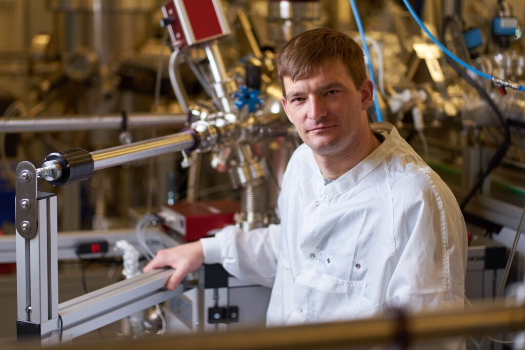
As laboratory director Michal Urbánek told us, the CEITEC Nano laboratories are part of the so-called Roadmap of Large Research Infrastructures of the Ministry of Education, Youth and Sports of the Czech Republic, which also provides the majority of their funding. “In return, the Ministry requires that we have as many users as possible across the broadest possible spectrum. This means that both students and researchers from around the world can access the laboratory under the same conditions,” explains Michal Urbánek. To become an authorized user, one must reserve time in advance on one of the 80 instruments available 24/7. Even so, the laboratories are constantly at full capacity. “To be able to accommodate more people, we’re working to streamline operations. We’re improving participant training so they manage their time well, and we try to interview and guide each researcher in advance so they use the infrastructure as efficiently as possible,” adds the head of the laboratories.
The annual fee for each user is 40,000 crowns, which helps offset operating costs to some extent. In addition, every registered user has the option to bring a visitor who can accompany them through the laboratories and observe the experiments. “For example, a doctoral student can bring a bachelor’s student, who can then get an idea of whether it’s worth their while to visit the laboratory. It is our priority to have as few bureaucratic obstacles as possible,” says Urbánek.
The CEITEC Nano research infrastructure is divided into four main sections: the nanofabrication laboratory, where nanostructures and nanocomponents are primarily produced; the nanocaracterization laboratory, where the manufactured samples are examined; the structural analysis laboratory focuses on investigating material structure, and in the X-ray microtomography laboratory, 3D mapping of nano-objects can be performed down to the sub-nanometer level. In 2023, an advanced chemistry laboratory was added to these cleanroom sections. “It’s no longer strictly a cleanroom laboratory, but it houses a lot of equipment for chemical analysis and chemical synthesis of samples,” explains the head of CEITEC Nano.
Since the facility opened, the instrumentation has been continuously modernized. “We secured several major renovation projects; the largest came from a special program for large research infrastructures. Our CzechNanoLab+ project became the most successful project in this call for proposals and received 361 million CZK earmarked for the modernization and innovation of equipment,” highlights Michal Urbánek, adding that the purchases are currently underway.
Cleanroom technologies were intended from the outset primarily for research in the field of microelectronics. Right behind the entrance door, we find an onsemi information board on the wall illustrating the semiconductor manufacturing process. “Most of our technologies are developed on silicon wafers, whether cut into pieces or left whole. On this board, we can see how the silicon wafers are first manufactured, how they are polished, and once the wafer is perfectly polished, various chips are produced on it during different stages of manufacturing,” comments Michal Urbánek. “We purchase the finished wafers and then perform what is known as lithography on them. This involves applying photoresists—either light-sensitive or electron-sensitive—and then using an electron beam or exposure through a mask to define shapes. The photoresists, which we expose and then develop, form a so-called mask for the next technological step, which is either material deposition or etching. “So we either remove material or deposit material only in the areas that are open in the mask. In this way, we deposit various layers on top of each other and produce functional devices,” explains the head of the chip manufacturing department.
Similarly, students can try their hand here, step by step, at fabricating a simple semiconductor structure on silicon, resulting in a semiconductor wafer with passive and active semiconductor components. “We organize various hands-on sessions where students from the Institute of Microelectronics manufacture their own boards with their own transistors and then measure them,” Urbánek explains. The main focus here, however, is research aimed at developing new technologies that are not commonly used in industry. “The industry uses semiconductor technologies, while we are trying to come up with other technologies that could replace or complement the semiconductor industry in the future,” explains Michal Urbánek. Scientists at CEITEC BUT are thus trying to design a completely different principle than the one used at onsemi. This could be, for example, a new approach to microprocessors or data transmission, or, conversely, the discovery of an interesting material that onsemi could use to replace their standard silicon carbide.
“In our research, we’re not trying to improve existing transistor technology. We’ll never be able to compete with big companies by inventing a better microprocessor. If you want to improve something in classic semiconductor technology, it costs a fortune, and it’s not worth competing with established firms. That’s why our research focuses on completely new approaches, such as photonic computers. These are areas that have much greater potential here—it’s a big unknown, and large companies haven’t poured money into it yet. So if we manage to achieve a breakthrough, there’s a chance that we’ll be pioneers in a certain technology in the Czech Republic,” concludes the head of the CEITEC Nano laboratory.
Source: News at BUT (written by Jana Novotná)
Photo: CEITEC BUT archive