The development of semiconductor materials for sustainable energy or modern organic electronics – all this is linked by one fundamental discipline: materials chemistry. At the Faculty of Chemistry, Brno University of Technology (FCH), its teaching and related research cover everything from a comprehensive understanding of chemistry through specific applications and technologies to industrial practice. The result is graduates in whom companies such as onsemi have a keen interest.
When Morten Meldal, winner of the 2022 Nobel Prize in Chemistry, was a guest on Czech Television’s Hyde Park Civilizace programme, he stated, among other things, that in a world made up of molecules, everything is connected to chemistry. This is also the view at FCH. “Chemistry is a vast field. It is in everything, even if it isn’t immediately apparent,” says František Šoukal unequivocally. He is the director of the Faculty’s Institute of Materials Chemistry and the programme coordinator for the Materials Chemistry and Technology programme, which is the subject of this discussion.
Sitting at the table with us is Martin Weiter, Vice-Rector for Research and Creative Activity at BUT, who originally trained as a microelectronics engineer but has devoted most of his professional life to chemistry, its teaching and research at the Faculty of Chemistry. “Chemistry is one of the fundamental sciences that explains how the world works, and it is only on this basis that applied disciplines in other fields are built, such as the materials sciences essential for mechanical or civil engineering. These disciplines cannot do without a foundation in chemistry.”
And specialists in semiconductor technology cannot do without them either. “From the perspective of the technological sequence, electrical engineering comes right at the very end of chip design. The preparation of material for chips is primarily a chemical, and partly a physical, matter. Chemists can design materials for chip production and synthesise them. Their role ends with the construction of complex electrical components. That is a matter for electrical engineers,” explains František Šoukal.

Chemistry, as a materials science, investigates the properties of materials at the atomic and subatomic levels, and this is very useful in the development and production of semiconductor materials, specifically those based on silicon or the more modern and technologically far more demanding silicon carbide. Production involves the preparation of single crystals, which are then cut into thin wafers that must be perfectly flat down to the level of individual atoms. This is where chemical-physical processes come into play, such as lapping (a special machining process that removes microscopic irregularities, ed.), polishing and the deposition of chip architecture. The whole process takes a matter of days or weeks, depending on the type of material and technology selected.
Graduates of the Faculty of Chemistry and Chemistry Technology (FCH) are increasingly finding roles in these industrial processes, and as the faculty representatives present emphasise, this is not a consequence of narrowly focused specialised training, but rather the opposite. “A chemistry student must first understand chemical principles in general – how nature is governed by them and how it functions as a result. Only on this basis can they pursue specific applications,” notes Martin Weiter, and František Šoukal adds: “The study programme must offer students the widest possible range of career opportunities. Our bachelor’s programme is therefore a traditional science course. It is based on a comprehensive understanding of chemistry, supplemented by certain technologies. In this respect, we are no different from other universities offering chemistry programmes. The differences emerge in the follow-up studies, where we place greater emphasis on technology, practical applications and links with industry.”
A concrete example of this strategy is the Materials Chemistry and Technology programme, which at the bachelor’s level generally prepares students for chemistry in all manner of material applications and related technologies – from construction materials through metals and polymers to functional materials such as semiconductors. Graduates gain a solid foundation in chemical and physical principles for further study in these fields, and are therefore well-suited to a wide range of industries.
Specialisation comes to the fore to a greater extent in the subsequent Master’s programme, which bears the same name as the Bachelor’s programme. This is achieved primarily through compulsory elective modules and subsequently through the topics of the Master’s thesis. “If someone knows they will be writing a thesis on semiconductors, they will not choose subjects specialising in polymers or construction materials in their Master’s studies, but will focus on structures, functional materials or nanotechnology,” confirms František Šoukal.
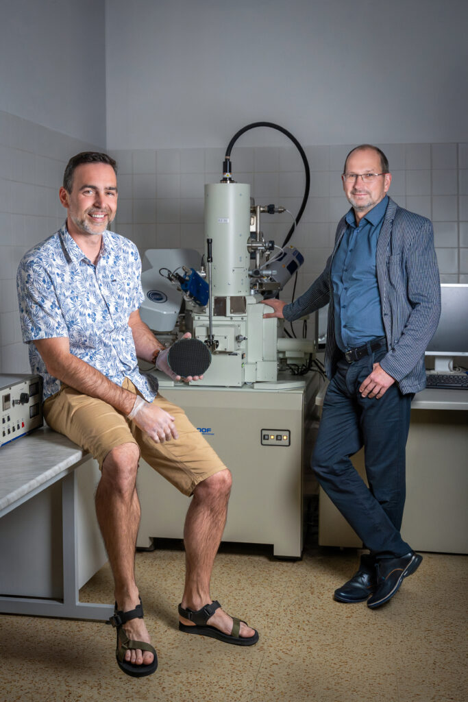
In 2010, BUT succeeded in project calls and acquired high-quality equipment for chemical and structural analysis, including cleanroom laboratory facilities. All this formed the basis of the FCH Materials Research Centre. This success has given the university a unique advantage and competitive edge, providing materials chemistry students not only with theoretical knowledge but also with extensive practical skills. This is reflected in the quality of undergraduate and postgraduate theses and in the interest shown by companies in FCH graduates.
“Some time ago, representatives from onsemi approached us with a proposal for collaboration. They provided us with a list of the competencies they expect from university graduates for their production needs. We found that within the Materials Chemistry and Technology programme, our graduates acquire such a set of knowledge, skills and competencies—whether chemical or physical—that we meet two-thirds of onsemi’s requirements. “The surprised reactions of the company’s representatives suggested that they had not yet encountered a single study programme that met their needs to such an extent,” smiles František Šoukal.
Both parties can now benefit from this collaboration. onsemi is keen to recruit specialists capable of handling, in particular, the highly demanding research and development of silicon carbide-based technologies. This material is increasingly being used in high-voltage applications, such as electric vehicles or photovoltaics, where silicon is not sufficient. “Silicon technologies have been developing for decades and all the fundamental issues have been resolved. In contrast, silicon carbide technology currently presents a major challenge. The synthesis and subsequent processing of single crystals, particularly due to their hardness, are extremely time-consuming and costly. The whole process requires a great deal of ingenuity, which is precisely what our graduates possess,” explains Šoukal. Whilst the company gains talented experts, the FCH has the opportunity to set topics for master’s theses and doctoral dissertations, the completion of which cannot be achieved without the use of the institute’s expensive industrial technologies. The result is a growing number of FCH representatives within the company – graduates, PhD students, undergraduates and interns – who are tackling the challenges of semiconductor material production through experimentation and research.
“We want to further develop our collaboration with onsemi. We will capitalise on the convergence of the company’s requirements and our graduates’ skills. This means we do not need to make any fundamental changes to our teaching or student preparation. Nevertheless, through re-accreditation, we are planning to innovate the study programme to reflect current trends under the new title ‘Materials for Industry, Medicine and Sustainability’, so that we can better appeal to prospective students. The most important thing, however, is to maintain quality,” adds Šoukal.
FCH leads the way in research and development of printed semiconductors
Another area the FCH focuses on in relation to semiconductor materials is organic semiconductors, also known as organic or plastic electronics. Examples of applications include OLED (Organic Light-Emitting Diode, ed.) displays in mobile phones, but they are also used in printed batteries, photovoltaics and smart clothing. The preparation of these materials involves a completely different process to that used for silicon semiconductors.

“The manufacturing process often exploits the fact that these materials can be used to create printing suspensions for material printing. Organic electronics can thus be printed on printing devices using a principle similar to that of paper newspapers, or via inkjet printing. You simply pour dissolved semiconductors – which are polymers in organic solvents – into the cartridge. In this way, you can print whatever is needed on a scale of kilometres and then process it for further use,” explains Martin Weiter.
These organic materials are not intended to replace existing silicon semiconductors in standard electronics. They are an alternative for specific applications. Several research avenues are currently being developed at FCH. One project, in collaboration with industry, focuses on the development of new transparent touchscreens used, for example, for menus in shops and restaurants. The experience gained is helping in the design of another project aimed at developing transparent photovoltaic systems. The aim is to create transparent flexible films which, when affixed to windows or a building’s façade, will absorb infrared radiation whilst simultaneously generating an electric current. The final area concerns the development of bioelectronic devices, intended primarily for regenerative medicine and the stimulation of various cell types.
Whilst research into semiconductors derived from inorganic chemistry relies on the faculty’s collaboration with industry, in the field of organic electronics, the focus of material development and research lies directly at the FCH. “The industry is still taking shape, and at the faculty we picked up on the development immediately after the Nobel Prize was awarded in 2000 for the discovery of conductive polymers. I promptly established a research group at FCH (the Laboratory of Organic Electronics and Photonics, ed.) and thus witnessed the very beginnings of the field at a European level. Thanks also to our membership of the Organic Electronics Association, we have managed to establish international contacts. In this field, we collaborate with leading global research centres, such as the universities of Bari, Linz and Oxford, from which we also welcome external examiners for our PhD theses,” concludes Martin Weiter.
Source: News at BUT (written by Petr Kubíček)
Photos: Václav Koníček