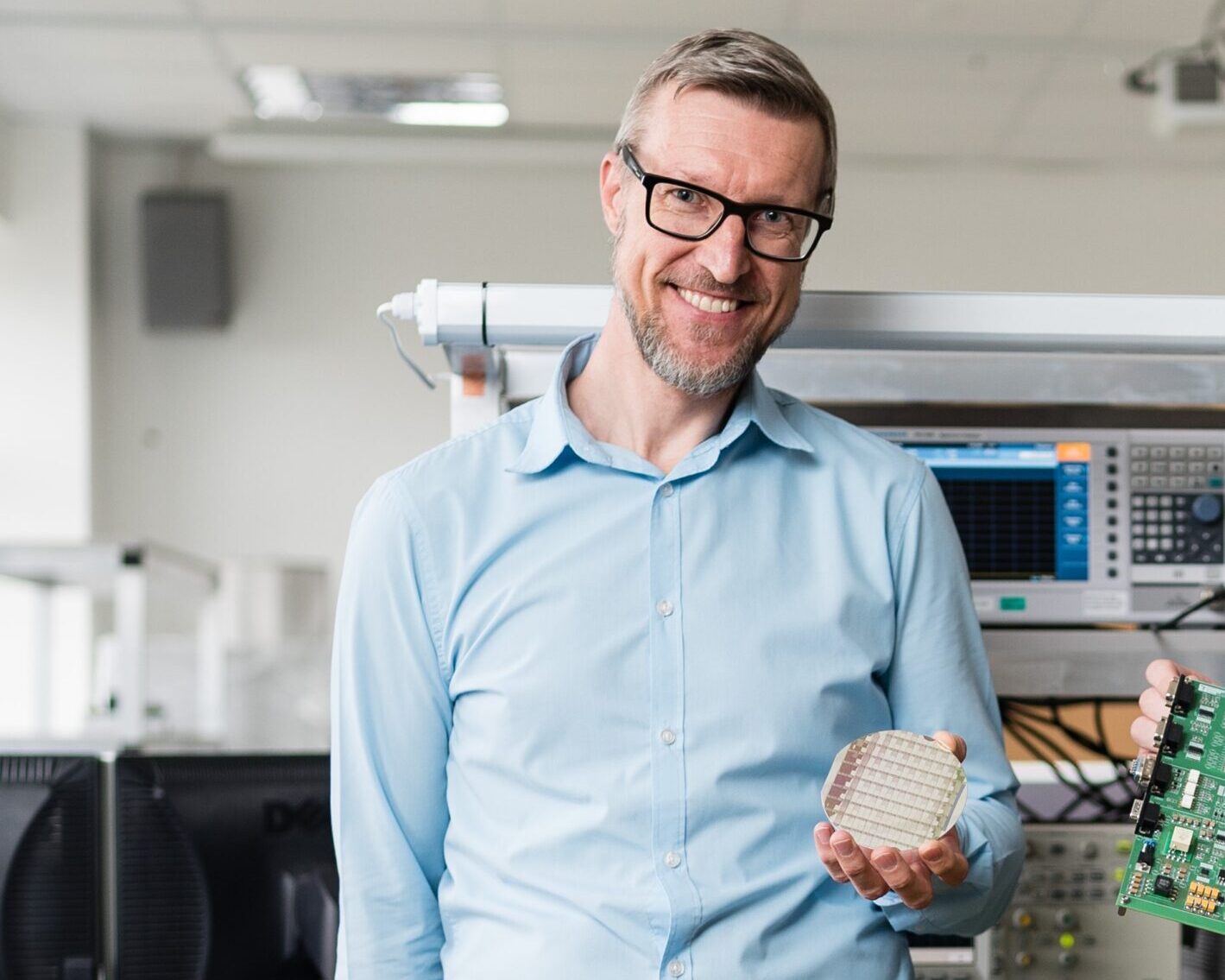
The history and present state of research and teaching in the field of semiconductors and chips at Brno University of Technology is intertwined with Jiří Háze’s memories of his studies at the Brno Faculty of Electrical Engineering, which he has not left since graduating. The current head of the Department of Microelectronics at the Faculty of Electrical Engineering and Communication (FEEC) is now BUT’s coordinator for chips and semiconductors under the BUT Semiconductor Technology Hub. The interview for the university magazine News at BUT was conducted by Jana Novotná.
History
Research and teaching of semiconductors and chips at BUT has its roots in the Department of Microelectronics at FEEC, which is celebrating its 45th anniversary this year. The institute, then still the Department of Microelectronics, was founded on 1st September 1980 at the former Faculty of Electrical Engineering. The workplace was created from the Department of Radioelectronics, where Jaromír Brzobohatý worked, and it was he who built the new department. “Professor Brzobohatý had experience in establishing the Institute of Electrical Engineering at the University of Sulaymaniyah in Iraq, so he was well equipped for the task. At the time of its establishment, the department focused on technologies and components for what was then small electronics,” explains Jiří Háze. As Jaromír Brzobohatý added, the current teachers at the institute, Radimír Vrba, Pavel Legát, Ivan Szendiuch, František Urban and Edita Hejátková, also helped significantly with the introduction and teaching of new subjects, and the departments of microelectronics at CTU Prague and STU Bratislava and the Tesla Rožnov and Tesla Lanškroun concern companies also provided great assistance.
The current head of the institute joined the faculty as a student in 1997. “I remember Professor Brzobohatý telling us about his travels in the Middle East and his years of activity in many advisory bodies, and thanks to that, we were able to get everything right in terms of legislation when building the department,” says Háze, recalling the merits of the doyen of the field, who also succeeded in laying the foundations for international mobility. “He had close ties with the Catholic University in Leuven and Ostend, Belgium, where they were already doing some impressive microelectronics work, including chip design. Even as an engineering student, when microelectronics was based in Údolní, I remember that teachers from Leuven used to come to us for guest lectures and our students went to Belgium for internships as part of the Tempus, Copernicus, Erasmus and other programmes. This established quite a fruitful cooperation,” recalls the head of the institute.
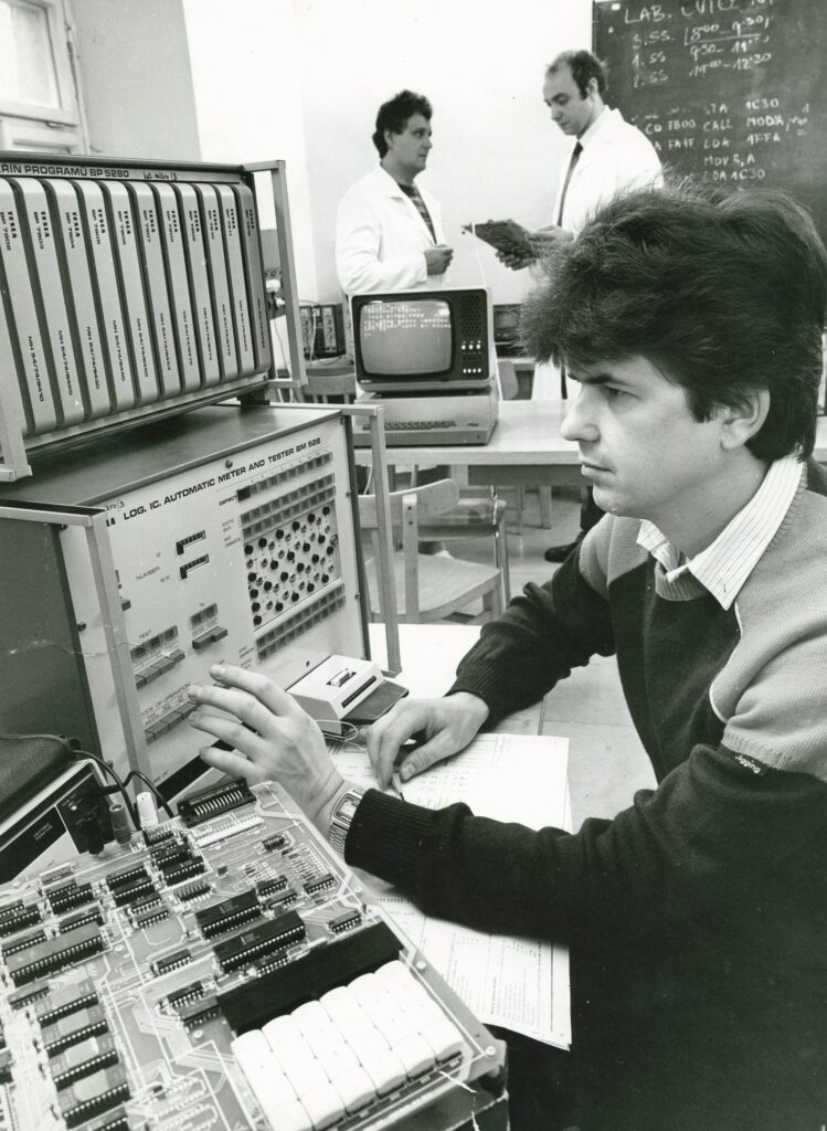 Jiří Háze did his diploma thesis under Radimír Vrba, who was the next head of the department after Jaromír Brzobohatý. Coming from the industrial sector, he had a number of useful contacts, which helped him to successfully acquire projects in which he also involved doctoral students. “At that time, chip design was already beginning to take off. In 2001–2002, when I was finishing my engineering studies, the first theses devoted to chip design appeared, thanks to the fact that those guys were in Leuven. At that time, the import of know-how, technical resources, software and tools took off, so it can be said that pure chip design has been done here for about 25 years. However, semiconductor technologies have a much longer history,” says Jiří Háze.
When he was looking for a topic for his doctoral thesis, he was put in touch with IMMS (Institute for Microelectronic and Mechatronic Systems) in Erfurt, Germany, where he then completed an internship lasting several months. “They offered me an interesting research topic in the field of converters and chip design, which then turned into a regular dissertation, and I continued with it until the end of my doctoral studies,” recalls the head of the institute. He completed his studies in 2005 and joined the institute, as did the current head of the chip design group, Lukáš Fujcik, and other graduates. “Then Roman Prokop joined the department, who had many years of experience at the then Alcatel (now onsemi) and who was a great addition to the chip design team. He had probably the most practical experience with design, so he took charge of managing all the software, licences and communication with IMEC in Belgium,” adds Háze.
Research
The institute’s research activities gradually focused on new areas. It is important to mention the launch of customer integrated circuit design, where the institute’s involvement in the pan-European Europractice project plays an important role. “It allows us to design chips up to the production documentation stage, which we generate and send to the aforementioned IMEC centre in Leuven. We receive back about 30 physical chip samples, which we use for our practical measurements and for the needs of colleagues from other institutes,” Háze points out.
In the field of chip design, the Department of Microelectronics is involved in a number of projects that end up being transferred to industry. “Perhaps the most striking example was our collaboration with the then-start-up company Codasip, where we worked with the company’s founder, Karel Masařík, through the entire process of designing his microprocessor. Since 2016, we have been focusing on electronics for space applications. Today, we are a direct supplier to the European Space Agency (ESA), for which we are currently working on several interesting projects – this is a huge credit to group leader Lukáš Fujcik,” the head of the institute proudly recounts. During 25 years of operation in the field, the Department of Microelectronics has designed and manufactured approximately 14 chips for various basic or applied research projects, either for its own laboratory use or for practical application, where a partner has used the chip in its products.
 In the field of technology, the institute focuses on new semiconductor materials with a so-called large bandgap, specifically silicon carbide. “These chips have the advantage of withstanding higher power loads than conventional silicon. They are used, for example, in electric cars, renewable energy sources, electric locomotives, and even space applications. The range of applications is quite large, and this is reflected in the massive interest of manufacturers around the world. Last year, onsemi announced huge investments in the production of silicon carbide-based chips,” recalls Jiří Háze.
Teaching
Chip design has been taught at the Institute of Microelectronics for a good twenty years and includes both classic technologies such as silicon and broadband materials. onsemi has also played a significant role in this. “Experts from onsemi come to us for regular lectures, and we have also revised the syllabi of several subjects in line with the company’s needs. We teach technology subjects in collaboration with the CEITEC Nano cleanroom laboratory. Fourth-year students can make simple semiconductor structures on silicon, which they must be able to encapsulate, mount on a board and measure their parameters. They learn what materials to use, how to design and manufacture a chip, test it and how to use it in a specific application,” Háze explains, adding: “Together with research and teaching at the Faculty of Mechanical Engineering (FME), the Faculty of Information Technology (FIT) and the Faculty of Chemistry (FCH), we offer expertise and knowledge in individual areas of the entire semiconductor ecosystem at BUT.”
Just a few years ago, almost no one outside the field knew about the Institute of Microelectronics. It was only after the crisis caused by the disruption of supply chains during the coronavirus pandemic and the need for independence from the American and Asian markets that the potential of BUT became apparent. Due to the need to ensure a sufficient number of qualified graduates, the Institute of Microelectronics felt the need to accredit a new study programme that would better reflect current and future trends in semiconductors. “On behalf of the Institute of Microelectronics, we agreed with companies on what they specifically needed, we involved physicists from the Faculty of Mechanical Engineering, we took some subjects from the Faculty of Information Technology and in a very short time we set up the study programme Chip Design and Modern Semiconductor Technologies, which was accredited for both bachelor’s and master’s degrees,” Háze points out. They used well-functioning subjects from old programmes as a basis and supplemented them with new subjects serving companies. The result is closer links with industry, guaranteed by lecturers not only from onsemi, but also from Tescan, Thermo Fisher Scientific and Codasip.
Thanks to these changes, the institute is now much more frequently invited to participate in projects. “We have submitted several projects that have been approved; for example, since last year we have had the Chips of Europe project focused on education. The old study programmes are coming to an end and new ones are starting in September, so we suddenly have over 300 applications,” says Jiří Háze, who estimates that at least half of those who have applied will enrol in the 2025–2026 academic year. “We are ready to welcome the first students to the new bachelor’s and master’s programmes in September, and I believe there will be around 200 of them.”
 This is also related to the need to strengthen the institute’s staff. “Recruiting people who are in short supply everywhere is really a challenge. The shortage of experts also makes it difficult for us to work on projects; I had to turn down two prestigious projects because we don’t have the staff capacity for them,” sighed the head of the institute. Even though the number of people at the institute has increased by ten over the past six months, it is still not enough. Nevertheless, Jiří Háze feels grateful that the Institute of Microelectronics, which until recently was struggling to make semiconductors and chip design part of the institute’s expertise, has suddenly found itself in the limelight. “I’m glad we persevered. The fact that we can design a chip, have it manufactured and get it back is unique. We are exceptional in this respect, and that sets us apart from others.”
Source: News at BUT (Jana Novotná)
Photo by Václav Koníček and the archives of the Department of Microelectronics, FEEC